
Waveshare Core3S500E XILINX FPGA Core Board
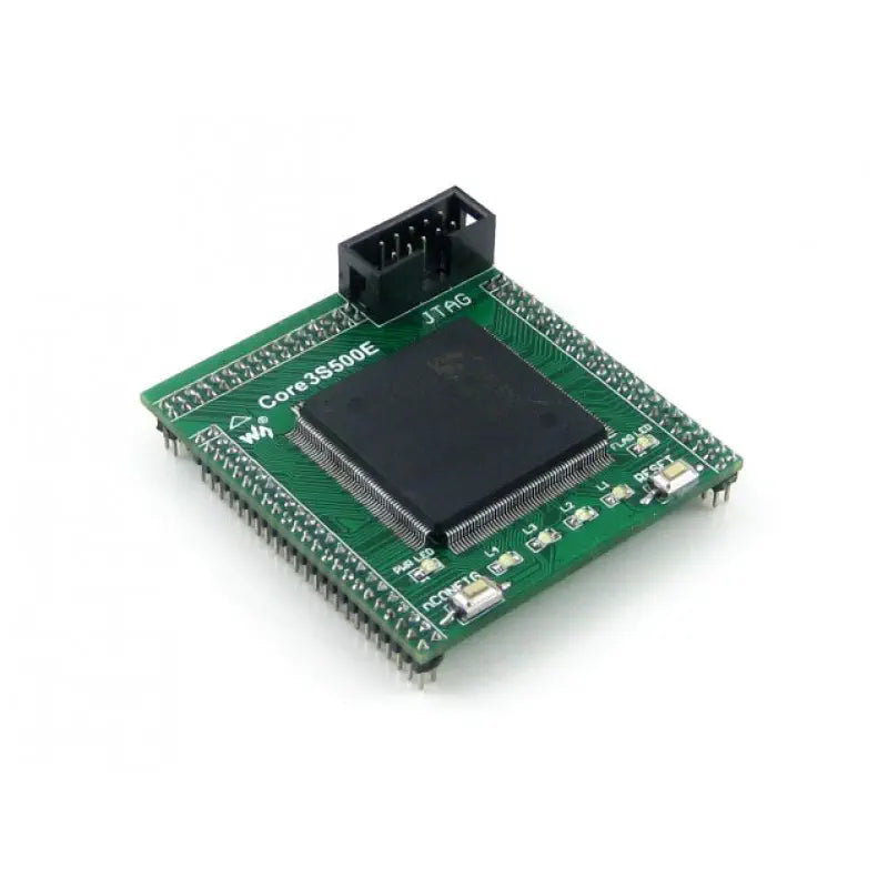
Description Waveshare Core3S500E XILINX FPGA Core Board Facilitates integration into various systems Supports operating voltages from 1.15V to 3.3V Provides 116 I/O ports and 500K logic elements Incorporates JTAG interface for debugging Includes 50M active crystal oscillator The Waveshare Core3S500E XILINX FPGA Core Board is an advanced development platform featuring the XILINX Spartan-3E chip, specifically the XC3S500E model. This board is designed to facilitate further expansion and integration into various application systems. It includes an integrated XCF04S FPGA basic circuit, complete with a clock circuit, and provides a comprehensive set of features for efficient development and debugging. The board is equipped with essential components such as a nCONFIG button, a RESET button, and four LEDs, all of which are accessible through pin headers. It also incorporates a JTAG interface for programming and debugging purposes. The 2.0mm header pitch design ensures compatibility with a wide range of application systems, allowing for seamless integration. The Core3S500E supports a range of operating voltages from 1.15V to 3.3V and operates at a frequency of 50MHz. It offers 116 I/O ports and 500K logic elements, making it suitable for complex FPGA applications. Additionally, the board includes a 50M active crystal oscillator and a power indicator, enhancing its functionality and usability. *Note: A separate debugger is required for JTAG debugging, as the board does not include integrated debugging functions. The motherboard and programmer/debugger are not included. View more What's Included 1x Waveshare Core3S500E XILINX FPGA Core Board Links Website Core3S500E, XILINX Core Board - Core3S500E Wiki Specifications Onboard 1 XCF04S chip Integrated FPGA basic circuit, including clock circuit Onboard nCONFIG button and RESET button Includes 4 LEDs All I/O ports accessible on pin headers Onboard JTAG debugging/programming interface 2.0mm header pitch design for application system integration Operating frequency: 50MHz Operating voltage: 1.15V to 3.3V Package type: QFP208 Number of I/Os: 116 Logic elements (LEs): 500K RAM: 360kb Digital Clock Managers (DCMs): 4 Supports JTAG for debugging/programming Includes AMS1117-3.3V voltage regulator Includes AMS1117-2.5V voltage regulator Includes AMS1117-1.2V voltage regulator Onboard XCF04S serial FLASH memory for code storage Power indicator present FPGA initialization indicator present nCONFIG button for re-configuring the FPGA chip, equivalent to power resetting 50M active crystal oscillator included JTAG interface for debugging/programming FPGA pins expander with VCC, GND, and all I/O ports accessible on expansion connectors for further expansion